- 您现在的位置:买卖IC网 > Sheet目录327 > HW-V5-ML561-UNI-G (Xilinx Inc)EVALUATION PLATFORM VIRTEX-5
�� �
�
�R�
�Appendix� A�
�FPGA� Pinouts�
�This� appendix� provides� the� pinouts� for� the� three� FPGAs� on� the� Virtex-5� FPGA� ML561�
�Development� Board.� The� toolkit� CD� shipped� with� every� ML561� contains� sample� UCFs� for�
�each� memory� interface.� These� UCFs� are� for� pinout� reference� only� and� do� not� include� other�
�constraints,� like� I/O� standards.�
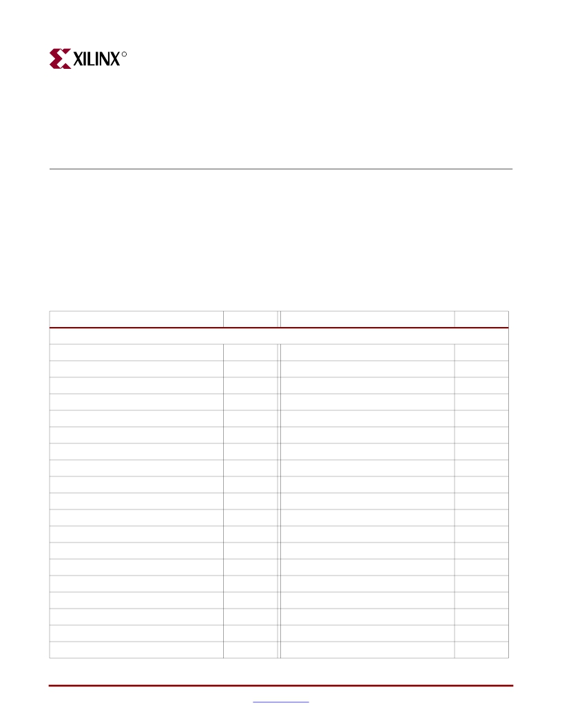
�FPGA� #1� Pinout�
��Table� A-1:�
�FPGA� #1� Pinout�
�Signal� Name�
�Pin�
�Signal� Name�
�Pin�
�DDR400� Component� Interface�
�DDR1_A0�
�DDR1_A1�
�DDR1_A10�
�DDR1_A11�
�DDR1_A12�
�DDR1_A13�
�DDR1_A2�
�DDR1_A3�
�DDR1_A4�
�DDR1_A5�
�DDR1_A6�
�DDR1_A7�
�DDR1_A8�
�DDR1_A9�
�DDR1_BA0�
�DDR1_BA1�
�DDR1_BY0_1_CS_N�
�DDR1_BY2_3_CS_N�
�DDR1_CAS_N�
�Virtex-5� FPGA� ML561� User� Guide�
�M32�
�L33�
�E33�
�E32�
�E34�
�F33�
�K32�
�K34�
�L34�
�J34�
�H34�
�H33�
�F34�
�G33�
�AK33�
�AK34�
�AB33�
�AC33�
�AC32�
��DDR1_CK1_N�
�DDR1_CK1_P�
�DDR1_CK2_N�
�DDR1_CK2_P�
�DDR1_CKE�
�DDR1_LB_BK11�
�DDR1_LB_BK11�
�DDR1_LB_BK13�
�DDR1_LB_BK13�
�DDR1_RAS_N�
�DDR1_WE_N�
�DDR1_DM_BY0�
�DDR1_DM_BY1�
�DDR1_DM_BY2�
�DDR1_DM_BY3�
�DDR1_DQ_BY0_B0�
�DDR1_DQ_BY0_B1�
�DDR1_DQ_BY0_B2�
�DDR1_DQ_BY0_B3�
�AJ34�
�AH34�
�AE34�
�AF34�
�AC34�
�N32�
�P32�
�AJ32�
�AK32�
�AB32�
�AD34�
�AG32�
�Y32�
�P34�
�G32�
�AP32�
�AN32�
�AN33�
�AN34�
�95�
�UG199� (v1.2.1)� June� 15,� 2009�
�发布紧急采购,3分钟左右您将得到回复。
相关PDF资料
I-JET
JTAG ARM DEBUGGING PROBE
IAC24A
INPUT MODULE AC 5MA 24VDC
IAC5EQ
INPUT MODULE AC 10MA 5VDC
IB8RM
SURGE SUPP 8OUT 12'CORD W/REMOTE
IBAR12-20T
SURGE SUPPRSSR 20A 12OUT RACKMNT
IBAR12/20ULTRA
SURGE SUPPRSSR 20A 12OUT RACKMNT
IBAR12ULTRA
SURGE SUPPRSSR 15A 12OUT RACKMNT
IBAR12
SURGE SUPPRSSR 15A 12OUT RACKMNT
相关代理商/技术参数
HW-V5-ML561-UNI-G-J
功能描述:EVALUATION PLATFORM VIRTEX-5 RoHS:是 类别:编程器,开发系统 >> 通用嵌入式开发板和套件(MCU、DSP、FPGA、CPLD等) 系列:Virtex®-5 LXT 产品培训模块:Blackfin® Processor Core Architecture Overview
Blackfin® Device Drivers
Blackfin® Optimizations for Performance and Power Consumption
Blackfin® System Services 特色产品:Blackfin? BF50x Series Processors 标准包装:1 系列:Blackfin® 类型:DSP 适用于相关产品:ADSP-BF548 所含物品:板,软件,4x4 键盘,光学拨轮,QVGA 触摸屏 LCD 和 40G 硬盘 配用:ADZS-BFBLUET-EZEXT-ND - EZ-EXTENDER DAUGHTERBOARDADZS-BFLLCD-EZEXT-ND - BOARD EXT LANDSCAP LCD INTERFACE 相关产品:ADSP-BF542BBCZ-4A-ND - IC DSP 16BIT 400MHZ 400CSBGAADSP-BF544MBBCZ-5M-ND - IC DSP 16BIT 533MHZ MDDR 400CBGAADSP-BF542MBBCZ-5M-ND - IC DSP 16BIT 533MHZ MDDR 400CBGAADSP-BF542KBCZ-6A-ND - IC DSP 16BIT 600MHZ 400CSBGAADSP-BF547MBBCZ-5M-ND - IC DSP 16BIT 533MHZ MDDR 400CBGAADSP-BF548BBCZ-5A-ND - IC DSP 16BIT 533MHZ 400CSBGAADSP-BF547BBCZ-5A-ND - IC DSP 16BIT 533MHZ 400CSBGAADSP-BF544BBCZ-5A-ND - IC DSP 16BIT 533MHZ 400CSBGAADSP-BF542BBCZ-5A-ND - IC DSP 16BIT 533MHZ 400CSBGA
HW-V5-PCIE2-UNI-G
功能描述:KIT DEV PCIEXPRESS GTX VIRTEX5 RoHS:是 类别:编程器,开发系统 >> 通用嵌入式开发板和套件(MCU、DSP、FPGA、CPLD等) 系列:Virtex® -5 产品培训模块:Blackfin® Processor Core Architecture Overview
Blackfin® Device Drivers
Blackfin® Optimizations for Performance and Power Consumption
Blackfin® System Services 特色产品:Blackfin? BF50x Series Processors 标准包装:1 系列:Blackfin® 类型:DSP 适用于相关产品:ADSP-BF548 所含物品:板,软件,4x4 键盘,光学拨轮,QVGA 触摸屏 LCD 和 40G 硬盘 配用:ADZS-BFBLUET-EZEXT-ND - EZ-EXTENDER DAUGHTERBOARDADZS-BFLLCD-EZEXT-ND - BOARD EXT LANDSCAP LCD INTERFACE 相关产品:ADSP-BF542BBCZ-4A-ND - IC DSP 16BIT 400MHZ 400CSBGAADSP-BF544MBBCZ-5M-ND - IC DSP 16BIT 533MHZ MDDR 400CBGAADSP-BF542MBBCZ-5M-ND - IC DSP 16BIT 533MHZ MDDR 400CBGAADSP-BF542KBCZ-6A-ND - IC DSP 16BIT 600MHZ 400CSBGAADSP-BF547MBBCZ-5M-ND - IC DSP 16BIT 533MHZ MDDR 400CBGAADSP-BF548BBCZ-5A-ND - IC DSP 16BIT 533MHZ 400CSBGAADSP-BF547BBCZ-5A-ND - IC DSP 16BIT 533MHZ 400CSBGAADSP-BF544BBCZ-5A-ND - IC DSP 16BIT 533MHZ 400CSBGAADSP-BF542BBCZ-5A-ND - IC DSP 16BIT 533MHZ 400CSBGA
HW-VID-KIT
功能描述:可编程逻辑 IC 开发工具 Lattice Video Interface Kit
RoHS:否 制造商:Altera Corporation 产品:Development Kits 类型:FPGA 工具用于评估:5CEFA7F3 接口类型: 工作电源电压:
HW-VL1
制造商:IDEC CORPORATION 功能描述:BARRIER
HW-VL2
制造商:IDEC Corporation 功能描述:COVER;HW FNGR SAFE CONTAC CVR 制造商:IDEC CORPORATION 功能描述:HW FNGR SAFE CONTAC CVR
HW-VL3
制造商:IDEC Corporation 功能描述: 制造商:IDEC Corporation 功能描述:Replacs TW-VL3 FNGR SAF
HWW-X030T-10015Z-H1
制造商:P-TEC 制造商全称:P-tec Corporation 功能描述:X30T RGB LED Wall Washers
HWW-X030T-10015Z-H2
制造商:P-TEC 制造商全称:P-tec Corporation 功能描述:X30T RGB LED Wall Washers